- 您现在的位置:买卖IC网 > Sheet目录3822 > PIC16F874A-I/PT (Microchip Technology)IC MCU FLASH 4K 20MHZ 44-TQFP
2003 Microchip Technology Inc.
DS39582B-page 137
PIC16F87XA
12.2
Comparator Operation
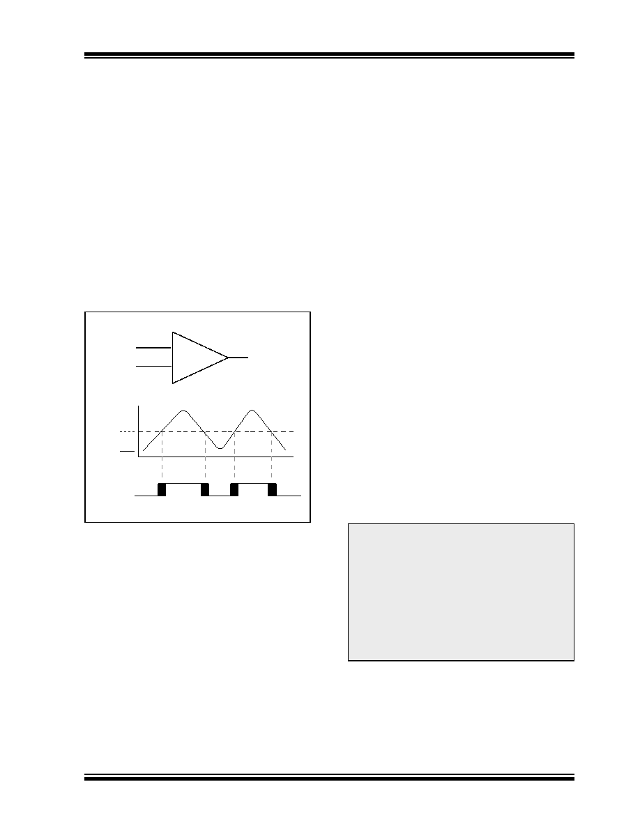
A single comparator is shown in Figure 12-2 along with
the relationship between the analog input levels and
the digital output. When the analog input at VIN+ is less
than the analog input VIN-, the output of the comparator
is a digital low level. When the analog input at VIN+ is
greater than the analog input VIN-, the output of the
comparator is a digital high level. The shaded areas of
the output of the comparator in Figure 12-2 represent
the uncertainty due to input offsets and response time.
12.3
Comparator Reference
An external or internal reference signal may be used
depending on the comparator operating mode. The
analog signal present at VIN- is compared to the signal
at VIN+ and the digital output of the comparator is
adjusted accordingly (Figure 12-2).
FIGURE 12-2:
SINGLE COMPARATOR
12.3.1
EXTERNAL REFERENCE SIGNAL
When external voltage references are used, the
comparator module can be configured to have the com-
parators operate from the same or different reference
sources. However, threshold detector applications may
require the same reference. The reference signal must
be between VSS and VDD and can be applied to either
pin of the comparator(s).
12.3.2
INTERNAL REFERENCE SIGNAL
The comparator module also allows the selection of an
internally generated voltage reference for the compara-
Module” contains a detailed description of the Compar-
ator Voltage Reference module that provides this signal.
The internal reference signal is used when comparators
are in mode, CM<2:0> = 110 (Figure 12-1). In this
mode, the internal voltage reference is applied to the
VIN+ pin of both comparators.
12.4
Comparator Response Time
Response time is the minimum time, after selecting a
new reference voltage or input source, before the com-
parator output has a valid level. If the internal reference
is changed, the maximum delay of the internal voltage
reference must be considered when using the compar-
ator outputs. Otherwise, the maximum delay of the
comparators should be used (Section 17.0 “Electrical
12.5
Comparator Outputs
The comparator outputs are read through the CMCON
register. These bits are read-only. The comparator
outputs may also be directly output to the RA4 and RA5
I/O pins. When enabled, multiplexors in the output path
of the RA4 and RA5 pins will switch and the output of
each pin will be the unsynchronized output of the com-
parator. The uncertainty of each of the comparators is
related to the input offset voltage and the response time
given in the specifications. Figure 12-3 shows the
comparator output block diagram.
The TRISA bits will still function as an output enable/
disable for the RA4 and RA5 pins while in this mode.
The polarity of the comparator outputs can be changed
using the C2INV and C1INV bits (CMCON<4:5>).
–
+
VIN+
VIN-
Output
VIN–
VIN+
Output
VIN+
VIN-
Note 1: When reading the Port register, all pins
configured as analog inputs will read as a
‘0’. Pins configured as digital inputs will
convert an analog input according to the
Schmitt Trigger input specification.
2: Analog levels on any pin defined as a dig-
ital input may cause the input buffer to
consume more current than is specified.
3: RA4 is an open collector I/O pin. When
used as an output, a pull-up resistor is
required.
发布紧急采购,3分钟左右您将得到回复。
相关PDF资料
PIC18F4480-I/PT
IC PIC MCU FLASH 8KX16 44TQFP
PIC16F876-20/SP
IC MCU FLASH 8KX14 EE 28DIP
PIC16F876-20/SO
IC MCU FLASH 8KX14 EE 28SOIC
DSPIC33FJ128GP802-E/SO
IC DSPIC MCU/DSP 128K 28-SOIC
PIC16C74B-04/P
IC MCU OTP 4KX14 A/D PWM 40DIP
PIC18LF242-I/SP
IC MCU FLASH 8KX16 A/D 28DIP
PIC18LF242-I/SO
IC MCU FLASH 8KX16 A/D 28SOIC
008017130000007
CONNECTOR RECEPTACLE 130POS
相关代理商/技术参数
PIC16F874A-I/PT
制造商:Microchip Technology Inc 功能描述:8BIT FLASH MCU SMD 16F874 TQFP44
PIC16F874A-I/PTG
功能描述:8位微控制器 -MCU 7KB 192 RAM 33 I/O Lead Free Package RoHS:否 制造商:Silicon Labs 核心:8051 处理器系列:C8051F39x 数据总线宽度:8 bit 最大时钟频率:50 MHz 程序存储器大小:16 KB 数据 RAM 大小:1 KB 片上 ADC:Yes 工作电源电压:1.8 V to 3.6 V 工作温度范围:- 40 C to + 105 C 封装 / 箱体:QFN-20 安装风格:SMD/SMT
PIC16F874AIP
制造商:Microchip Technology Inc 功能描述:
PIC16F874AT-E/ML
功能描述:8位微控制器 -MCU 20MHz 4K Flash RoHS:否 制造商:Silicon Labs 核心:8051 处理器系列:C8051F39x 数据总线宽度:8 bit 最大时钟频率:50 MHz 程序存储器大小:16 KB 数据 RAM 大小:1 KB 片上 ADC:Yes 工作电源电压:1.8 V to 3.6 V 工作温度范围:- 40 C to + 105 C 封装 / 箱体:QFN-20 安装风格:SMD/SMT
PIC16F874AT-E/PT
功能描述:8位微控制器 -MCU 20MHz 4K Flash RoHS:否 制造商:Silicon Labs 核心:8051 处理器系列:C8051F39x 数据总线宽度:8 bit 最大时钟频率:50 MHz 程序存储器大小:16 KB 数据 RAM 大小:1 KB 片上 ADC:Yes 工作电源电压:1.8 V to 3.6 V 工作温度范围:- 40 C to + 105 C 封装 / 箱体:QFN-20 安装风格:SMD/SMT
PIC16F874AT-I/L
功能描述:8位微控制器 -MCU 7KB 192 RAM 33 I/O RoHS:否 制造商:Silicon Labs 核心:8051 处理器系列:C8051F39x 数据总线宽度:8 bit 最大时钟频率:50 MHz 程序存储器大小:16 KB 数据 RAM 大小:1 KB 片上 ADC:Yes 工作电源电压:1.8 V to 3.6 V 工作温度范围:- 40 C to + 105 C 封装 / 箱体:QFN-20 安装风格:SMD/SMT
PIC16F874AT-I/ML
功能描述:8位微控制器 -MCU 7KB 192 RAM 33 I/O RoHS:否 制造商:Silicon Labs 核心:8051 处理器系列:C8051F39x 数据总线宽度:8 bit 最大时钟频率:50 MHz 程序存储器大小:16 KB 数据 RAM 大小:1 KB 片上 ADC:Yes 工作电源电压:1.8 V to 3.6 V 工作温度范围:- 40 C to + 105 C 封装 / 箱体:QFN-20 安装风格:SMD/SMT
PIC16F874AT-I/PT
功能描述:8位微控制器 -MCU 7KB 192 RAM 33 I/O RoHS:否 制造商:Silicon Labs 核心:8051 处理器系列:C8051F39x 数据总线宽度:8 bit 最大时钟频率:50 MHz 程序存储器大小:16 KB 数据 RAM 大小:1 KB 片上 ADC:Yes 工作电源电压:1.8 V to 3.6 V 工作温度范围:- 40 C to + 105 C 封装 / 箱体:QFN-20 安装风格:SMD/SMT